Von Neumann Processor Architecture - 12/10/18
The Hungarian-American mathematician Johnny Von Neumann devised the standard for processor architecture which is an elementary part of the majority of all computer processors today; he conceived of a system by which program data and instructions are stored in the same memory - a computer's random access memory, or RAM, which is split into sectors, each with a unique address. This type of processor architecture makes use of the fetch-decode-execute cycle when carrying out operations. It is this cycle on which this article will mainly focus.
Below: a photograph of Johnny Von Neumann (image from Wikipedia):
Below: a summary layout of the CPU, RAM, and connecting buses:
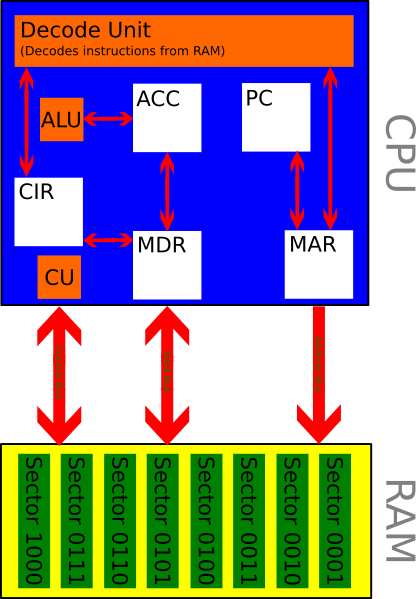
The central processing unit of a computer contains the following key components:
The CPU and RAM are connected by three buses. A bus is a set of parallel wires linking two components in close proximity on a computer motherboard. These are the three buses:
At the start of a cycle, the address stored in the program counter is transferred to the memory address register. The memory then waits for a "read" signal from the control unit over the control bus and, once the signal has been received, the memory sends the contents of the desired memory sector (whose address is stored in the MAR) to the memory data register over the data bus to the memory data register. This value is transferred to the CIR. At this point, the value in the PC is incremented by 1 so that it points to the next memory sector from which data is to be fetched.
At this stage, the data in the CIR is decoded by the decode unit into the operator and the memory address of the data to be used by this instruction. This address (now different to the value stored in the PC) is copied to the MAR and the necessary data obtained from the RAM sector over the data bus. This new data is stored in the MDR and copied to the ACC. The instruction is finally executed, carrying out the necessary operations on the value in the ACC.